Big Advance Reported in Metasurfaces for Antireflective Optics Coatings
June 22, 2022
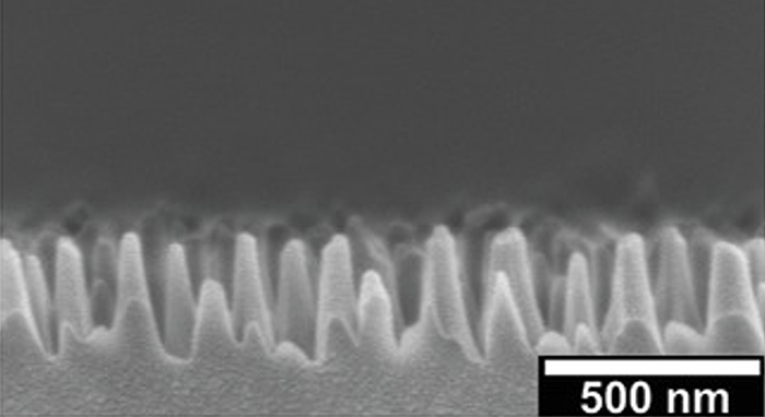
 A scanning electron microscope cross-section of a metasurface (MS) fabricated for broadband anti-reflective applications.
 LLNL researchers have reported a significant advance in broadband antireflective (AR) coatings applied to optics using nanostructure metasurface technology. The research was featured in the cover story of the May 18 edition of Advanced Optical Materials.
Metasurfaces, and more broadly metaoptics, with ultrathin metasurface properties that differ from those within the bulk of the material, are used to overcome limitations in optic processing advances. The ability to produce adjustable, nanoscale (billionth of a meter) surface features with patterning has been demonstrated to satisfy large-area AR applications at a given ultraviolet wavelength and for broadband needs.
AR coatings play an instrumental role in display panels, laser and optical/imaging systems, as well as in renewable energy such as solar cells. Fields that stand to benefit from AR coatings with improved performance, mechanical durability, or broadband/broad angle operation include directed energy for additive manufacturing, renewable energy, and lithographic applications.
The paper, first published online April 14, cited an advanced nanoparticle masking approach to fabricate two metasurfaces: a vertical sidewall nanofeature metasurface (MS) for AR applications at 351 nanometers (nm), and a sloped sidewall MS designed for broadband AR applications.
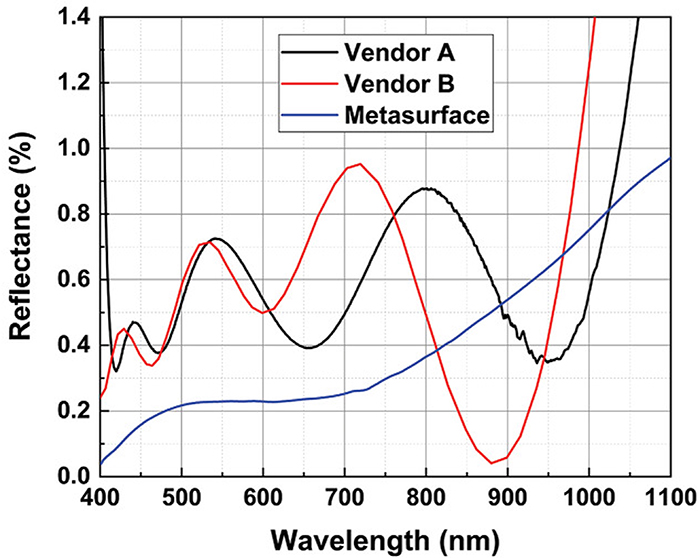
For the 351-nm MS, reflectance was measured at 0.127 percent. In the sloped sidewall MS, reflectance was measured at less than 0.25 percent over 400 to 700 nm and less than 1 percent over 400 to 1,100 nm. LLNL research scientist Eyal Feigenbaum, the Principal Investigator for the study, noted that the challenge is bigger for shorter wavelengths since the metasurface features must be made much smaller than the wavelength with good enough control of the features’ size.
“To the best of the authors’ knowledge, this is the first demonstration of a broadband AR capable of this performance,” the researchers said in the paper. “The tunability of these structures, with a parameter space spanning even more remarkable designs such as broader bands and acceptable angles, coupled with high laser-induced damage durability and mechanical robustness, displays the strength of metasurfaces for AR applications.”

LLNL staff research scientist Nathan Ray, the paper’s lead author, said, “The fact that we were able to fabricate a large-scale AR metasurface (for this demonstration on inch-wide window, about 600 square millimeters) with that low of reflectance is also a big deal, as it is typically difficult to fabricate AR layers from metasurfaces because layers such as these have traditionally been written feature-to-feature, and an area as small as 1 square millimeter requires about 100 million features.
“The presented process, in principle, can be scaled up to fabricate meter-sized optics with minimal impact on the processing time due to the self-assembly of the etching mask and at-once etching process,” he said. “This scalability is necessary to meet the requirements of high-power laser systems like NIF.”
What differentiated this from previous demonstrations was the masking technology developed by the Lab.
“This broadband AR is significant relative to previous demonstrations due to the processing limitations we were able to overcome,” Ray said. “By using an advanced etch mask technology, we were able to etch deeper and obtain more sloping than was previously possible, which allowed us to fabricate a broadband AR layer that is more broad than what is commercially available today.
“Furthermore, we were able to decrease the average reflectance relative to both our previous demonstrations and commercially available broadband AR coatings,” he added.
The masking technology is part of the four-step Metasurface Laser Printing (MSLP) process that produces adjustable, nanoscale (billionth of a meter) surface features with patterning across substrates.
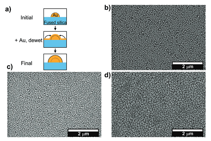
 (Top left) Schematic of nanoparticle growth. A gold seed is in the top panel; the middle panel depicts a gold film deposited over the seed with arrows denoting the direction of gold diffusion during dewetting, and the bottom panel depicts the resultant nanoparticle. Panels b) to d) display electron micrographs of the first, fourth, and seventh deposit/dewet cycles using initial gold films of 5 nanometer thickness.
Ray also noted that this demonstration also highlights the uniformity of the optical path difference (OPD) of the metasurface across the sample. For traditional optics the OPD nonuniformity results mainly from surface height nonuniformity, whereas for the metasurface the dominant mode is a result of effective index variation in the sample.
“An open question about our process had been the ability to which we could fabricate a uniform effective index of refraction,” he said, “and here we demonstrate that the equivalent surface roughness of our structure is comparable to that of a high-quality optical window.
“The ability to tune MS nanofeatures opens opportunities for designing other properties of the MS, such as mechanical, thermal, and hydrophobicity properties, which, in concert with the optical properties, paves the way to countless optical elements surface designs,” the authors concluded. “These results show great promise to impactfully expand the application space of scalable substrate-engraved metasurfaces.”
The work was conducted under the LLNL Laboratory Directed Research and Development (LDRD) Office as “Glass-Engraved Meta-Optics (GEM) for High- Power Lasers.”
Along with Feigenbaum and Ray, LLNL colleagues Jae-Hyuck Yoo and Hoang T. Nguyen were co-authors of the paper.
More Information:
“Researchers Develop Novel Antireflective Metasurface for Laser Optics,” NIF & Photon Science News, June 4, 2020
“Metasurface Laser Printing Could Improve NIF Optics,” NIF & Photon Science News, October 29, 2019
—Jon Kawamoto
Follow us on Twitter: @lasers_llnl


