Researchers Develop Novel Antireflective Metasurface for Laser Optics
June 4, 2020

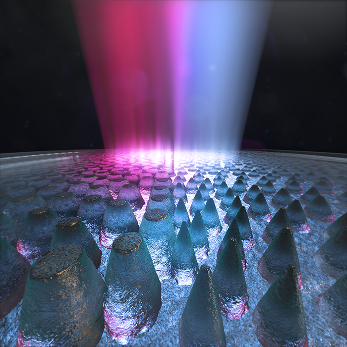
Lawrence Livermore National Laboratory (LLNL) scientists have discovered a new method to add an antireflective metasurface (ARMS) layer on laser optics glass that’s so durable, it can survive getting “smooshed.” The relatively simple technique represents a substantial advancement that could benefit the National Ignition Facility and a wide range of lasers and imaging optics.
Tests also found the ARMS layer’s structure, created with an LLNL-developed technique that transforms the optic’s surface into the structured metasurface engineered for the desired wavelengths, does not exacerbate the growth of damage normally caused by high-power laser light, according to a paper published in the May edition of The Optical Society journal Optica.

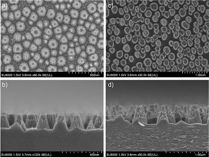
Note: magnifications vary.
“These metasurfaces show great promise to impactfully expand the applications of high-power lasers, ranging from compact new particle and X-ray sources, renewable energy, directed energy, and fundamental light-matter interaction exploration,” the researchers said.
The paper details research seeking alternative ways to create an antireflective (AR) metasurface for NIF optics without adding different materials to the glass or introducing potential defects that could diminish performance and durability. The research was funded by LLNL’s Laboratory Directed Research and Development (LDRD) program and endorsed by the Laboratory’s NIF & Photon Science Directorate.
“This original work presents the first demonstration — to the best of our knowledge — of an anti-reflective engraved meta-surface which has both superior mechanical and laser-induced durability, as well as high flexibility in tailoring its optical reflection properties,” said LLNL research scientist Eyal Feigenbaum, who leads this LDRD.
This work builds on the team’s previous research enabling Metasurface Laser Printing (MSLP) (see "Metasurface Laser Printing Could Improve NIF Optics").
An antireflective layer is one of the most critical components of a laser optics system. The layer can help maximize energy transmission and help protect the system from damaging stray or deflected light. That’s especially important for NIF, the world’s largest and most energetic laser system, which has more than 7,500 meter-sized optics and 26,000 smaller optics.
Easy to Implement
Currently, two main types of AR coatings in use are: a sol-gel coating layer mainly used for fused silica substrates (with limitations such as frequency bandwidth, uniformity, and environmental stability); and multi-dielectric coatings (which have a lower laser damage performance). The coatings can become another source of failure for the laser system, such as from laser-induced damage.
“The strength of this new method is that we are etching directly into the substrate so that this AR layer is basically a reforming of the topography of the glass,” said LLNL scientist Nathan Ray, the paper’s lead author. “We haven’t added any material to it. The beauty of this process is it’s quite simple and easy to implement.”
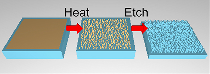
In the four-step ARMS process, an ultrathin layer of gold film is deposited on the optic surface. In a furnace which gives a uniform heat deposition over the area, the film self-assembles into metal nanoparticles in a process called dewetting, leaving a nano-patterned mask. A reactive ion beam then etches nanoscale pillar-like features into the optic, after which removal of the mask from the surface leaves a monolithic glass structure.
Other methods using a mask-less process had been creating random patterns of AR nano-scale features that are more needle-like, a shape with less design flexibility that is more likely to break when force is applied to the top.
The ARMS process provides a way to determine the nano-feature shapes and patterns. The researchers used 2-inch round, 1-milimeter thick fused silica substrates and gold film layers with thicknesses of 7.5 and 10 nanometers for the masks.

The team found they could adjust the thickness of the gold film layer, the temperatures used during different points of the dewetting process, and the depth of the etchings to create the types of nanostructures they wanted.
“It was interesting finding you can control the dewetting process with temperature, which was not something that was obvious,” Feigenbaum said. “We learned how to choose the temperature and thickness of the film layer to get a different nanoparticle mask for a particular design. Then we etch using reactive ion-beam etching directed from the top for a prescribed amount of time to dig through this nano-particles mask.
“If we stop the etching process before the gold mask starts to erode, we end up with a very straight sidewall,” he said. “If we continue the etching process, it starts to tilt the sidewalls. Depending how much we continue etching, we can control the angle of the sidewalls from completely straight to completely cone-shaped.”
Adjusting the slope of the nanostructures’ walls adjusts their antireflective properties to function for a larger span of laser wavelengths.
The method is effective because of “its simplicity, once you know the process-parameters to be used,” Ray said. “By controlling the mask, we can control the structures we get after etching. We can fabricate little pillars or we can make them little cones akin to nanoscale pyramids, with a geometry that is very robust.”

To test the layer’s durability, Ray tried “many different kinds of punishment,” starting with a sonication bath. “Then I squished it with my thumb and dragged a wipe over the surface,” he said. “That was not very methodic, but I just wanted to test what would happen.”
Under a microscope, the optic looked “completely unscathed, so we had to go to much higher pressures before we started to damage it,” he said. He then measured pressure using an indenter, a device with a fine tip about 2 to 20 times the width of a human hair. That revealed an even more interesting phenomenon.
Even at higher pressures, the nanostructures “bounced back into shape. They would completely recover,” Feigenbaum said. “We were pleased and surprised to see that if you continue applying pressure, they get smooshed and not break. That said, at large enough pressures they will break, of course.”
The structures survived pressures a minimum of two orders of magnitude higher than if someone placed their fingerprint on the glass. From a practical standpoint, this means the AR layer would improve the ability of laser optics to stand up to the contact of cleaning and incidental handling.
“I was surprised by the magnitude of the pressures they could withstand,” Ray said.
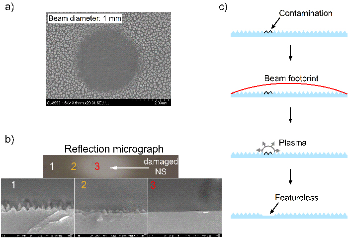
Moreover, tests showed the ARMS itself does not introduce damage in the optic. Typically, laser-induced damage from a microscopic contaminant on the glass can cause fractures that grow with subsequent shots. With the ARMS, when damage is initiated when the laser light hits a contaminant on the AR layer, a plasma plume melts the underlying AR nanostructures. That creates a featureless spot that could be about 500 times smaller than the laser beam’s footprint.

“Because these features have already melted and flattened out, the damage site doesn’t grow,” Ray said.
The ARMS layer wouldn’t prevent the usual laser damage seen in glass, but potential future damage wouldn’t be caused by an AR coating.
“The glass is the glass, so you cannot get beyond the glass damage point,” Ray said. “The goal is to get as close to that as you can.”
The researchers will next try to further improve the performance and durability on larger scale samples. They hope this technology could eventually be employed on meter-scale optics used by NIF and other high-power lasers being developed.
Ray and Feigenbaum are joined on the paper, “Substrate-engraved antireflective nanostructured surfaces for high-power laser applications,” by LLNL colleagues Jae-Hyuck Yoo, Hoang Nguyen, Michael Johnson, Salmaan Baxamusa, and Selim Elhadj.
—Benny Evangelista
Follow us on Twitter: @lasers_llnl


