Science & Technology - 2016
December
NIF Experiments Boost Computer Chip Manufacturing
Increasing Carrying Capacity of Fiber-Optic Cables
More than 3.4 billion people are connected to the Internet, placing ever-increasing demand on the telecom industry to provide bigger, better, and faster bandwidth to users. LLNL researchers have taken an important step in addressing that need by developing a new type of optical fiber amplifier that could potentially double the information-carrying capacity of fiber-optic cables.
Most of the data for the Internet travels on fiber-optic cables, which are made up of bundles of threads that transmit laser light. As the fiber gets longer, however, power is lost due to attenuation. In the late ’80s and early ’90s, researchers discovered that they could mitigate this loss by developing inline fiber-optic amplifiers.
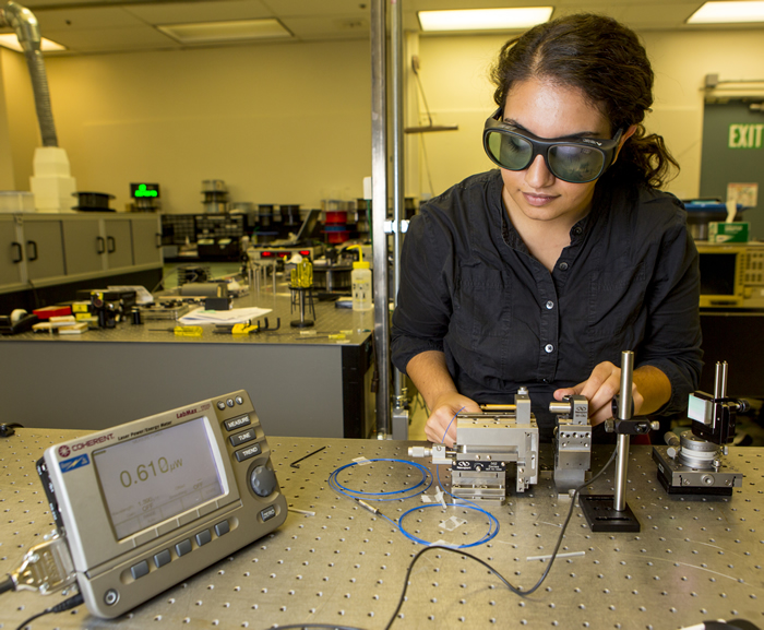 NIF & Photon Science postdoctoral researcher Leily Kiani tests a new optical fiber that could double the bandwidth of fiber-optic cables. Credit: Jason Laurea
 At the time, lasers operated at a wavelength of 1.3 microns, or 1300 nanometers (nm). No optical amplifiers were developed, however, that worked well in that region. Researchers were able to develop an amplifier at 1.55 microns, or 1550 nm, so laser transmission systems were switched to match. At the same time, they discovered that inline optical amplifiers allowed them to amplify many different lasers at one time, a discovery that increased the information carrying capacity of a single optical fiber from 155 megabits a second to more than one terabit a second. While this was a huge increase, it is still a limited amount of information, requiring many cables to transmit.
Flash forward 25 years. The Livermore team was working on neodymium-doped optical-fiber lasers, which lase at 1330 nm (1.33 microns), 1064 nm (1.064 microns) and 920 nm. The team built a custom optical fiber that suppressed lasing at 1064 nm and amplified light preferentially at 920 nm. In the course of testing the 920-nm laser, the team observed in the fluorescent spectra that the fiber also showed signs of amplification at 1400-1450 nm—a wavelength that never worked previously.
Previous fiber amplifiers did not suppress lasing at 1064 nm and were also observed to suffer from an effect known as excited-state absorption in the 1330-nm region. This effect actually causes the fiber loss to increase when pump light is applied—the opposite of the desired effect, which is to generate optical gain.
The team then redesigned the fiber to suppress laser action at both 1064 nm and 920 nm. This new fiber, which completely eliminates the potential for lasing at 920 nm or 1064 nm, can now only provide gain on the 1330-nm laser transition. Excited-state absorption still precludes amplification at 1330 nm, but the laser line amplifies light across a large range of wavelengths.
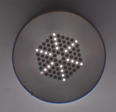 End-face view of the new optical fiber. The fiber has an outer diameter of 126 microns and the observable features are 6.6 microns apart. The center spot is doped with neodymium ions, the same dopant used in NIF’s lasers, but the material is fused silica glass instead of phosphate glass. The bright dots are GRIN (gradient-index) inclusions, and the dark spots are fluorine-doped fused silica, which have a lower refractive index than undoped fused silica.
 The team discovered that from 1390 nm to 1460 nm there is significant positive optical gain, and this new fiber generates laser power and optical gain with relatively good efficiency. This discovery opens up the potential for installed optical fibers to operate in a transmission region known as E-band, in addition to the C and L bands where they currently operate—effectively doubling a single optical fiber’s information-carrying potential.
“The key missing component for operating a telecom network in this wavelength region has been the optical fiber amplifier,” said Jay Dawson, deputy program director for DoD Technologies in the NIF and Photon Science Directorate. “What we’ve done is effectively create something that will look and feel like a conventional erbium fiber amplifier, but in an adjacent wavelength region, doubling the carrying capacity of an optical-fiber amplifier.”
The amplifiers would potentially allow telecom companies to more heavily leverage their installed base of equipment, requiring less capital investment than new cable—resulting in expanded bandwidth and lower costs to the end user. Installation of new cable is expensive; a service provider must not only purchase new cables, but also undergo the large expense of digging trenches to install the new cable.
“By using the fiber we’ve developed, you could build a set of optical fiber amplifiers that would look virtually identical in technology to the fiber amplifiers that already exist,” Dawson said. “Instead of having to lay another expensive cable, you could install these new amplifiers in the same buildings as the current amplifiers, resulting in twice as much bandwidth on the current cables.”
“To me, that’s what is exciting about it,” he added. “It’s something that no one has previously been able to do, and the potential is there to really make a big difference.”
Initially started as a Laboratory Directed Research and Development (LDRD) project (see “New Horizons for High-Power Fiber Lasers”), the research is now funded by the LLNL Industrial Partnerships Office (IPO)’s Innovation Development Fund (IDF). IDF uses internal monies to fund interesting, but early-stage, projects that are expected to have commercial application.
“This appeared to be a significant discovery which may solve a problem in the telecommunications industry, which is a large and important market, but more R&D was needed,” said Michael Sharer, IPO manager for technology commercialization. “The IDF committee felt that this was an important project to fund from this standpoint.”
In addition to Dawson, researchers on the project are Graham Allen, Diana Chen, Matt Cook, Parker Crist, Reggie Drachenberg, Victor Khitrov, Leily Kiani, Mike Messerly, Paul Pax, and Nick Schenkel.
NIF Experiments Boost Computer Chip Manufacturing
High energy density (HED) physics experiments on NIF are contributing to the development of next-generation semiconductors.
ASML, a leading provider of computer chip manufacturing equipment, is tapping LLNL’s expertise in lasers and plasma physics and the Lab’s high-performance computing capability to perform complex, large-scale modeling and simulation to improve the performance of extreme ultraviolet (EUV) lithography. Switching to EUV light sources will make it easier to produce the smaller transistors desired for next-generation semiconductor fabrication plants.
The combined resources will enable efficient and economical testing of new approaches targeted at further optimizing conversion efficiency, increasing source power, and minimizing tin debris in microchip manufacturing.
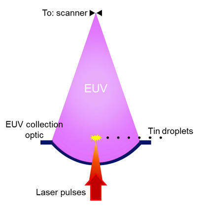
EUV light is generated when a high-intensity carbon dioxide laser pulse hits droplets of tin, heating them to become plasma (ionized gas). The plasma emits EUV radiation that is then collected and transferred to a microlithography scanner, where it is used to expose silicon wafers. To increase EUV power, ASML researchers turned to high-fidelity computer simulations to better understand the physics of laser-produced plasmas and fill in the gaps for challenging lab experiments.
“Merging expertise, we demonstrated that computer codes developed by LLNL can accurately simulate ASML’s experimental data from its EUV light source,” said Steve Langer, computational physicist and project lead for LLNL. “Now that the simulation results and experimental data are aligned, we better understand the physics of EUV generation and can start to gain insight into what makes the light source perform well or poorly.”
Langer said the researchers used LLNL’s HYDRA and ALE-AMR 3D multi-physics simulation codes to simulate EUV experiments conducted by ASML. “Both codes have been used to simulate a large number of NIF experiments,” he said. “Comparisons between simulations and NIF experiments led to a number of changes that improved the codes.”
Langer pointed out that the ASML experiments use a lower laser intensity and a longer laser wavelength than is used in NIF experiments. “The wide variety of NIF experiments that were simulated put the two codes in much better shape to deal with the jump to new laser conditions,” he said. “Both codes owe a large debt to earlier LLNL codes that were used since the start of ICF (inertial confinement fusion) experiments.”
In order to successfully build an accurate and predictive simulation, ASML engaged with LLNL’s High Performance Computing Innovation Center (HPCIC) and the NIF & Photon Science Directorate’s Advanced Photon Technologies (APT) Program in a cooperative research and development agreement (CRADA) to gain access to world-class supercomputers, software and deep domain knowledge, as well as experience in the application of advanced computing technologies. Livermore HPC capabilities and familiarity with HED physics occurring in laser-driven fusion experiments at NIF proved directly applicable to the technical challenges encountered in ASML’s advanced EUV lithography development.
“This is a wonderful example of how expertise and capabilities across LLNL can be successfully brought together with leading industry experts to intensely focus on advancing photon sources of great importance to the commercial sector and broader society,” said Craig Siders, commercial technology development leader in the APT Program.
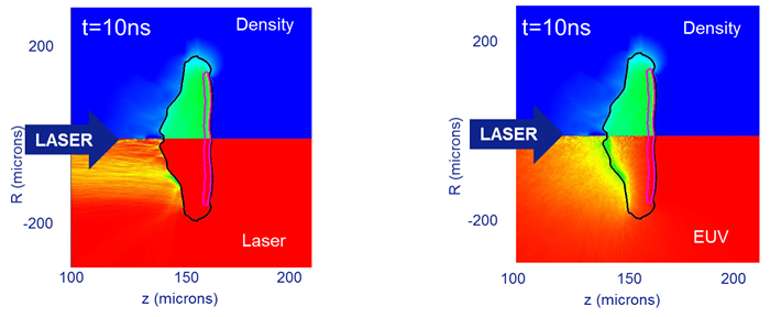 Simulations enable ASML to look at plasma in a way that is not possible with experimental data, like the above 2D maps. Here, ASML takes a slice through a density map at a specific instance in time and uses it to better visualize how the laser rays enter the plasma and interact with different densities in the target (i.e., how the rays are refracted and bent out of the plasma). ASML can then use it to better visualize where the EUV is produced within the plasma and create a better mental picture of EUV production.
 “While we have world-class strength in laser-plasma codes built up over decades of ICF research,” he said, “it’s LLNL’s people, who daily take on the hard challenges of simulating cutting–edge HED experiments on NIF, that make them work.
“It’s our people who envision how to simulate these incredibly complicated physical systems on some of the most powerful computers in the world, and who turn it around to make an even more capable generation of simulation codes and machines—and test those on the world’s most powerful laser, NIF. It’s that broad Livermore team that makes this work. And in this case, we get to help the whole process improve again by working closely with industry and the LLNL HPCIC to literally make the processor chips smaller, faster, and more efficient.”
ASML’s San Diego R&D and manufacturing facility specializes in the production of light sources used within microlithography scanners. ASML’s complex systems image a pattern on a silicon wafer, building up billions of transistors and circuit elements layer by layer, to make integrated circuits, or microchips, for the semiconductor industry. Its next-generation EUV technology will enable chipmakers to increase the number of transistors and significantly improve the performance of supercomputers and electronics.“We anticipate our research partnership with LLNL will help us quickly zoom into the most promising technology development approaches, and thus shorten the time to market for future high-power EUV sources,” said Michael Purvis, senior scientist at ASML. “We’ve already extended our knowledge of tin plasmas through our joint modeling efforts that promise to help advance EUV power for high-volume manufacturing environments.”
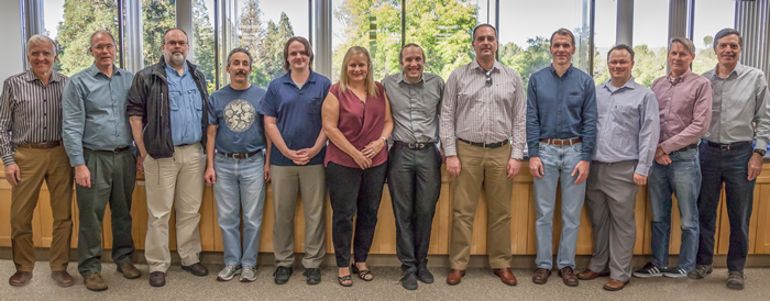 Researchers involved in the EUV lithography collaboration (from left): Dave Eder, Wayne Miller, Craig Siders, Howard Scott, Kevin Gott (LBNL), Alice Koniges (LBNL), Aaron Fisher, Chris Kavouklis, Jave Kane, Tony Link, Scott Wilkes, and Steve Langer. Not pictured: Fred Hartemann. Credit: Clayton Dahlen
 “Our collaboration with ASML is just one example of how leading-edge companies can partner with Lawrence Livermore’s world-class HPC resources to advance technologies that stand to broadly benefit the computing industry as a whole, as well as help sustain U.S. leadership in science and technology,” added Fred Streitz, director of the HPCIC.
Computer scientists at the National Energy Research Scientific Computing Center at Lawrence Berkeley National Laboratory are leveraging their expertise in laser plasma modeling software development to support the LLNL-ASML CRADA.
ASML is one of the world’s leading manufacturers of chip-making equipment. ASML’s guiding principle is continuing Moore’s Law toward ever smaller, cheaper, more powerful and energy-efficient semiconductors. For more information about the ASML-LLNL collaboration, see “Living in a parametric space as a scientist” and “Affecting progress from a parametric space as a scientist.” For another example of the synergy between NIF experiments and LLNL supercomputer simulations, see “Coming to Grips with Chaotic Plasma Behavior.”
Along with Langer, researchers participating in the collaboration were Dave Eder, Aaron Fisher, Fred Hartemann, Jave Kane, Tony Link, Wayne Miller, Howard Scott, and Scott Wilks of LLNL and Kevin Gott and Alice Koniges of Lawrence Berkeley National Laboratory.


