Papers and Presentations - 2017
May
NIF Laser Technology Could Revolutionize Metal 3D Printing
HAPLS Takes the Spotlight at International Conference
Limiting Laser-Driven Optics Contamination
LLNL researchers have developed new techniques for mitigating a major source of damage to the optics in NIF and other high-energy laser systems—a source largely created by the laser itself.
In a research paper in the May 15 issue of Optics Express, the researchers reported that almost all of the observed damage to NIF’s fused silica optics is due to contamination from laser-driven particle sources. They said their findings demonstrate that in a high-energy system-level environment such as NIF, laser-driven sources are the most significant sources of particle contamination and must be controlled.
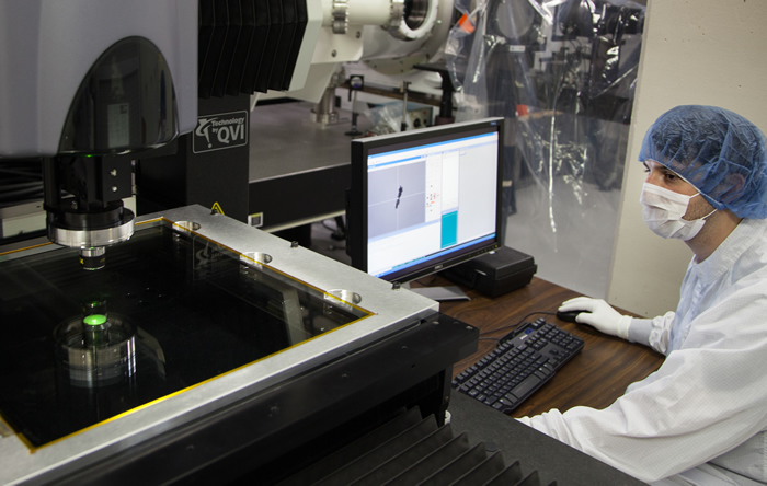 Electro-optic technician Ryland Plummer identifies input surface bulk eruptions, or damage sites, on a NIF disposable debris shield (DDS) that was removed from a NIF beamline after a shot. The eruptions on the DDS can introduce silica glass fragments into the beamline, contaminating other optics. Credit: James Pryatel
 Optics damage occurs when flaws, defects, and contaminants absorb laser light and trigger a reaction that creates a damage crater in the optic. Surface damage sites are initially tiny, usually a fraction of the size of a human hair. Under continued illumination by the laser, however, these “precursor” sites can grow; after several shots, the area of a site can become large enough to disrupt the performance of the laser beam on the target, limiting the operating energy of the laser system as well as the optic’s lifespan.
In the Optics Express paper, lead author Jeff Bude and colleagues noted that years of research into the causes of optics damage have been successful in reducing and mitigating sub-surface damage and precipitates of trace impurities introduced during optics manufacturing and processing. New processing techniques such as the Advanced Mitigation Processes, known as AMP2 and AMP3, have made significant improvements in damage resistance in laboratory tests of small optics treated with the AMP processes.
In large laser systems, however, “the full benefit of these improvements has not been fully realized,” the researchers said. “Many hundreds of damage sites can occur on optics exposed to several (five or more) shots” at fluences (energy densities) of eight joules per square centimeter—which is lower than NIF’s full operating energy of 10 J/cm2.
The laser-driven particle contamination on NIF was traced to two main sources: glass fragments from inexpensive and untreated disposable debris shields (DDSs) designed to intercept target debris during NIF shots; and debris that occurs when reflected light from the exit surface of the multipurpose grating debris shields (GDSs) create a highly focused beam of light known as a “ghost” that damages stray-light-absorbing glass just above the exit surface of the GDS. The two debris shields are the final optics in the integrated optics modules (IOMs) before NIF’s laser beams enter the Target Chamber.
“Every time we shot the laser,” said Jeff Bude, lead author of the report, “it was damaging the IOM” and generating debris that landed on the GDS. The debris particles created thousands of potential damage sites on the GDSs, many of which, when exposed to the high-energy ultraviolet light from NIF’s laser beams, eventually grew large enough to render the optic useless. “The debris-caused damage was limiting the performance of the inherently damage-resistant AMP-treated optic,” Bude said.
To address these issues, the researchers treated the exit surfaces of the grating debris shields with an LLNL-developed anti-reflective coating (see “Next-Generation NIF Optics Boost Energy and Limit Damage”); and they developed a damage-resistant fused silica debris screen to insert in the IOM and protect the GDS and other upstream optics from contamination by the disposable debris shield.
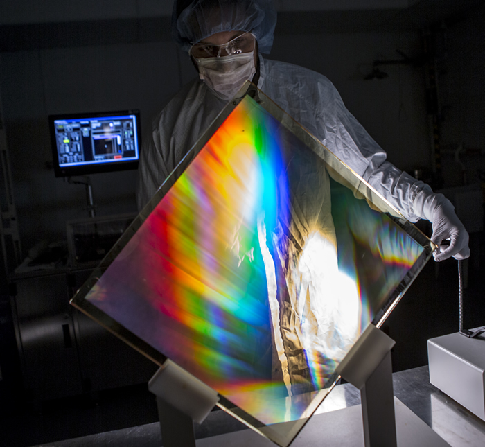 Researcher Marcus Monticelli tests a new anti-reflective grating debris shield. Credit: Jason Laurea
 “Understanding and solving this problem,” Bude said, “was a result of sustained research and development on the impact of various types of debris on laser damage and from novel experiments on NIF and in offline laser test laboratories.”
While optics damage is managed on NIF through a robust optics recycling process called the Optics Recycle Loop, the researchers said reducing initial damage levels would lead to improved efficiencies for optic repair and replacement, increase the number of high-fluence shots which could be taken, and significantly increase the maximum operating fluence of the laser.
“Mitigation of laser-driven particle sources allows demonstration of the full potential of the AMP process improvements,” they said, “eliminating more than 98 per cent of the damage to large-scale fused silica optics at three-nanosecond fluences near nine J/cm2. These mitigations are currently being employed on all NIF’s 192 beamlines. This work shows that the elimination of laser-driven particle sources is an important consideration for any high-fluence laser system.”
Joining Bude on the paper were LLNL researchers Wren Carr, Phil Miller, Tom Parham, Pam Whitman, Marcus Monticelli, Rajesh Raman, David Cross, Brian Welday, Frank Ravizza, Tayyab Suratwala, Jim Davis, Matt Fischer, Ruth Hawley, Henry Lee, Ibo Matthews, Mary Norton, Mike Nostrand, Diana VanBlarcom, and Stanley Sommer.
More Information
“Looking for Trouble on Optical Surfaces,” Science & Technology Review, April-May 2017
“Sleuthing an Optical Mystery,” Science & Technology Review, January-February 2015
NIF Laser Technology Could Revolutionize Metal 3D Printing
An award-winning technology originally developed to smooth out and pattern NIF’s high-energy laser beams now can be used to 3D-print metal objects faster than ever before, according to a new study by LLNL researchers.
A team of Lab scientists reported the finding in an Optics Express article published online on May 10. The new method—Diode-based Additive Manufacturing (DiAM)—uses high-powered arrays of laser diodes, a Q-switched (pulsed) laser, and a specialized laser modulator developed for NIF to flash-print an entire layer of metal powder at a time, instead of raster scanning with a laser across each layer as with conventional laser-based powder-bed fusion additive manufacturing systems.
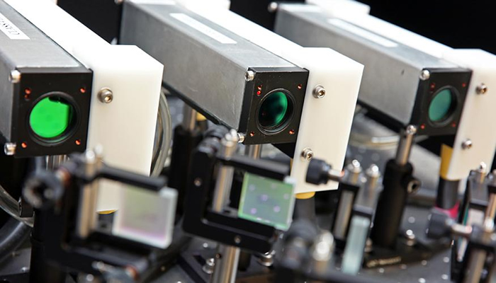 In Diode-based Additive Manufacturing, laser light is sourced by a set of four diode laser arrays and a pulsed laser. Credit: Kate Hunts
 The result, the researchers said, is the potential for large metal objects to be printed in a fraction of the time needed for metal 3D printers on the market today, expanding possibilities for industries requiring larger metal parts, such as aerospace and automotive manufacturers. The combination of speed and degree of design flexibility afforded through the DiAM method, the team concluded, is potentially “far beyond” that of current powder-bed fusion-based systems.
“By cutting the print time and having the ability to upscale, this process could revolutionize metal additive manufacturing,” said Ibo Matthews, the LLNL scientist heading the research and the paper’s lead author. “Hypothetically, a one-cubic-meter build would take 10 years of raster-scanned illumination time using current methods, but would only require hours to weeks with DiAM, because you can image large areas of build all at once. Printing with a grey-scaled image may also allow you to reduce residual stress, because you can tailor the thermal stresses spatially and temporally.”
The “magic” of the process, Matthews said, is the implementation of a customized laser modulator called an Optically Addressable Light Valve (OALV), which contains a liquid crystal cell and photoconductive crystal in series. Much like a liquid-crystal-based projector, researchers explained, the OALV is used to dynamically sculpt the high-power laser light according to pre-programmed layer-by-layer images. But unlike a conventional liquid-crystal projector, the OALV is un-pixelated and can handle high laser powers.
The technology originally was designed for and installed in NIF as part of the LEOPARD (Laser Energy Optimization by Precision Adjustments to the Radiant Distribution) system, in collaboration with Meadowlark Optics in Colorado and CEA, the French Alternative Energies and Atomic Energy Commission. LEOPARD was deployed in 2010 and won an R&D 100 award in 2012. In NIF, the OALV is used to optimize the profile of the laser beams and locally shadow and protect optics subjected to higher intensities and fluences, or energy densities.
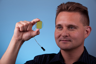 John Heebner holds an Optically Addressable Light Valve; the OALVs are in each of the 48 programmable spatial shapers forming the NIF LEOPARD system.
 With LEOPARD, NIF electronically protects regions of its beams containing potentially threatening flaws on its final optics, as identified by the Final Optics Damage Inspection (FODI) system. This enables NIF to continue firing until the schedule allows those optics to be removed, repaired, and reintroduced into the beamline.
The team that first demonstrated the light valve could be used for printing parts was initially led by James DeMuth, a former LLNL researcher. John Heebner, the LLNL scientist who led the development of the OALV, described its use in metal 3D printing as a “natural synergy.”
“The DiAM project marries two technologies that we’ve pioneered at the Lab—high-power laser-diode arrays and the OALV,” Heebner said. “Given that we put all this time and development into this light valve, it became a natural extension to apply it to this project.
“We went through some calculations and it was clear from the outset that it would work (with 3D printing),” he said. “The ability to change a serial process to a parallel process is critical to ensuring that as parts increase in complexity or size that the patterning process speed can be increased to catch up.”
Beside the potential to produce larger parts, using such a valve results in imaging quality that rivals and could exceed today’s metal 3D printers, and the ability to fine-tune gradients in the projected image means better control over residual stress and material microstructure, researchers said.
With DiAM printing, the laser light is sourced by a set of four diode laser arrays and a nanosecond (billionth of a second) pulsed laser. It passes through the OALV, which patterns an image of a two-dimensional “slice” of the desired 3D part. The images go from a digital computer file to the laser in a two-stage liquid-crystal modulation process.
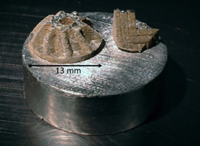 First demonstration of DiAM wide-area photolithographic printing of metal layers using an optically-addressable light valve. For each build—impeller (left) and LLNL logo—successive layers were built using a stitching approach which allowed additional efficiency to be achieved. Alternatively, scaling up overall dimension can be achieved by simply adding diodes and expanding optics, up to the two-joule energy limit of the pulsed laser system.
 In the first stage the images are sourced from a digitized CAD (computer-aided design) model and imprinted on a low-power blue LED (light-emitting diode) source using an ordinary pixelated liquid-crystal projector. In the second stage the blue images activate the OALV’s photoconductive layer, creating local conductive patches (where blue light is present) that transfer voltage to its liquid-crystal layer. This enables the low-power blue images to modulate the high-power laser beam. The beam is then directed onto a build plane, printing the entire metal layer at once.
For the study the researchers used tin powder, successfully demonstrating the printing of two small 3D models, an impeller (a small turbine blade structure) and the LLNL logo.
While speeding up the metal additive process was a main driver for pursuing the technology at LLNL, the larger build size potentially could have significant value for the Lab’s core mission of stockpile stewardship, the researchers said. The laser diodes, which provide most of the energy compared to the pulsed laser system, are also cheap to purchase, so such a system would be more cost-effective than fiber-laser-based machines on the market today.
LLNL’s Laboratory Directed Research and Development program funded the research. Lab scientists Gabe Guss and Reggie Drachenberg played a central role in producing the parts, with contributions from Josh Kuntz and Eric Duoss.
HAPLS Takes the Spotlight at International Conference
NIF & Photon Science physicist Emily Sistrunk Link highlighted LLNL’s recent success in developing the world’s highest-energy diode-pumped femto-petawatt (quadrillion-watt) laser in an invited talk on May 18 at a major international conference of the laser industry.
 Emily Sistrunk Link
 Her presentation at the Conference on Lasers and Electro-Optics (CLEO) in San Jose described the record-breaking aspects of the High-repetition-rate Advanced Petawatt Laser System (HAPLS). HAPLS was designed and built by the Laboratory for use at the European Extreme Light Infrastructure Beamlines facility (ELI Beamlines) in the Czech Republic.
The talk focused on the short-pulse capabilities of the HAPLS laser that promise to break new ground with pioneering science at the ELI Beamlines facility. HAPLS set a world record for diode-pumped petawatt lasers when it achieved its final commissioning milestone in December, with energy reaching 16 joules and a 28-femtosecond (quadrillionths of a second) pulse duration (equivalent to about 0.5 petawatt per pulse) at a 3.3-Hz (3.3 times a second) repetition rate.
The first all-diode-pumped petawatt-class laser offers the average powers required for secondary source applications. Sistrunk Link’s talk discussed the utilization of HAPLS’ short-pulse beamline to provide a robust, turn-key high peak- and average-power laser, and the use of the laser system to enable high-fidelity data collection at a high rep rate.
Sistrunk Link, a member of the Advanced Photon Technologies program, started with the Lab as a postdoc three years ago and was part of the team that built the laser and is now taking it apart to ship to the Czech Republic. She and other members of the team will help scientists there reassemble and integrate the laser system into the ELI Beamlines facility, where it will be ramped to its full design performance—one petawatt at a 10-Hz repetition rate.
At the CLEO conference, many fellow scientists came up to Sistrunk Link and excitedly asked what she and her team were going to do next. With a gleam in her eye, she responded, “We have lots of ideas for the future here.”
Hers was one of 150 invited talks out of some 2,000 technical presentations at the conference on lasers, optical materials and photonic devices that has been meeting for more than 30 years and attracts close to 5,000 attendees from more than 60 countries.
“Talking about HAPLS in this context is great,” said Sistrunk Link. “Part of the excitement surrounding our work here is that all this was only conceived three years ago, designed, built and now on its way out.”


