Papers and Presentations - 2016
January
Nine Varieties of Nanoporous Gold on a Single Chip
Visualizing High-energy Electrons in Fast-ignition Targets
Fast ignition (FI) is an alternative approach to conventional inertial confinement fusion that involves separating the compression and heating phases of the implosion, using a more stable compression followed by a short burst of localized heating. By separating these two aspects, the fuel can be compressed isochorically (without a central hotspot), reducing the fuel density requirements or increasing the mass of fuel that can be compressed and potentially leading to higher gain. The heating pulse in electron FI is generated by a separate short-pulse petawatt (quadrillion-watt) laser that creates an intense, MeV (million-electron-volt) electron beam that deposits its energy into the compressed core.
Fast ignition requires efficient heating of pre-compressed high-density fuel by an intense relativistic electron beam produced from laser–matter interaction. Understanding the details of electron-beam generation and transport is crucial for FI.
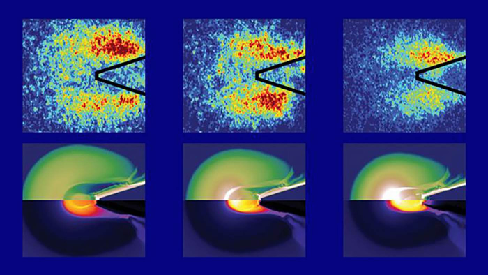
In a paper published in the Jan. 11 issue of Nature Physics, an international team of researchers reported on the first visualization of fast electron spatial energy deposition in a laser-compressed cone-in-shell FI target. Led by Farhat Beg and Charlie Jarrott of UC San Diego and Mingsheng Wei of General Atomics, the team included LLNL scientists Hui Chen, Tilo Döppner, Mike Key, Harry McLean, and Prav Patel. The research was facilitated by doping the shell with copper and imaging the K-shell x-ray radiation (the K shell is the electron orbit closest to the nucleus). The experiments were conducted at the OMEGA Laser Facility at the University of Rochester’s Laboratory for Laser Energetics (LLE) as part of the National Laser Users Facility program that provides academic access to the LLE facilities for basic science research.
 In the fast-ignition experiments, high-energy electrons were generated when the laser beam hit the inside of the cone. The top row shows the experimental images and the bottom row depicts simulations performed by LLE scientist Andrey Solodov, a co-author on the Nature Physics paper. By integrating copper into the fuel capsule, the researchers were able to obtain images of K-shell radiation from the copper and analyze the flow of energy.
 The experiments show the spatial distribution of the fast electrons and reveal key parameters affecting energy coupling. Successful visualization of relativistic electrons within the FI scheme opens the door for optimizing the target design by providing a more direct way to infer energy coupling.
The technique guided experimental designs that showed a significantly improved laser-to-core coupling energy efficiency of 7 percent. This represents a factor-of-four improvement over previous results for relativistic electron energy coupling to a compressed plastic shell, and is currently the highest coupling efficiency ever reported on the OMEGA Laser Facility. This proven experimental platform could be extended to megajoule-scale laser facilities such as NIF.
Jarrott, the lead author of the study, recently joined LLNL as a postdoc. The experiments reported in the paper were conducted by Jarrott during his graduate research at UC San Diego. Other institutions involved in the work were Osaka University, the University of Bordeaux, and the University of Nevada at Reno.
Nine Varieties of Nanoporous Gold on a Single Chip
Nanoporous gold (np-Au), a porous metal useful for applications in energy and biomedical research, is produced through an alloy corrosion process known as dealloying that generates a characteristic three-dimensional nanoscale network of pores and ligaments.

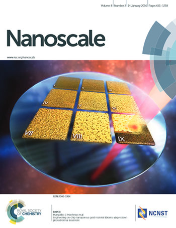
In the cover article in the Jan. 14 issue of Nanoscale, a journal published by the Royal Society of Chemistry, LLNL researchers and their collaborators from UC Davis describe a method for creating a library of varying np-Au morphologies on a single chip via precise delivery of tunable laser energy.
Laser micro-processing (e.g. micromachining), a highly controllable and precise method to cut, anneal, and modify materials, provides spatial and temporal control while imposing energy near the surface of the material. “Traditional heat application techniques for the modification of np-Au are bulk processes that cannot be used to generate a library of different pore sizes on a single chip,” the researchers said. “Laser micro-processing offers an attractive solution to this problem by providing a means to apply energy with high spatial and temporal resolution.”
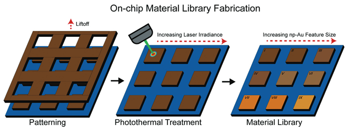
The researchers used finite element multiphysics simulations to predict the effects of continuous-wave vs. pulsed laser mode and thermal conductivity of the supporting substrate on the local np-Au film temperatures during photothermal annealing. Following the guidance of the simulations, they were able to fabricate an on-chip material library consisting of 81 np-Au samples of nine different morphologies for use in the parallel study of structure–property relationships.
 Schematic illustrating the suggested process to be used for the fabrication of on-chip np-Au (brown) material libraries supported on silicon or glass (blue) using laser-based precise photothermal treatment to selectively anneal each np-Au pattern, resulting in an altered feature size (denoted by color change) on each pattern.
 “These libraries have the potential to drastically increase the throughput of morphology interaction studies for np-Au, specifically in applications such as surface enhanced Raman spectroscopy (SERS), high capacity lithium ion batteries, cell-material interaction studies for neural interfaces, analytical biosensors, as well as nanoscale material science studies,” the researchers said. “Ultimately this work sets the foundation for understanding laser-based annealing of porous thin film materials. The fabrication of single chip material libraries has the potential to increase the throughput of material interaction testing in many disciplines through easy single-chip material screening libraries.”
“This project successfully assembled a very diverse team, ranging from biosensor application engineers to nanomaterial and optical materials scientists, to create a useful interfacial engineering solution,” said LLNL’s Ibo Matthews, corresponding author for the paper.
Lead author Christopher Chapman, a UC Davis graduate student, was joined on the paper by UC Davis colleagues Ling Wang and Erkin Seker and by LLNL researchers Juergen Biener, Monika Biener, and Matthews. The research was supported by UC lab fees, the National Science Foundation, and the National Institutes of Health.


