How NIF Inspired Groundbreaking 3D Metal-Printing Technology
June 21, 2021
A seminar at Stanford University, the decades-long quest for fusion energy, and an innovative technique for protecting NIF’s optical components from laser damage were the inspiration for a new high-speed 3D manufacturing technology that’s about to enter the market.
Developed by an industrial partnership between LLNL and Seurat Technologies Inc. of Wilmington, Massachusetts, the technology, called Large-Area Pulsed Laser Powder Bed Fusion (LAPBF) Area Printing™, has the potential to revolutionize metal additive manufacturing (AM). Companies requiring larger metal parts, such as aerospace and automotive manufacturers, are among the industries that could benefit from industrial metal printers with unparalleled speed and resolution.
The technologies enabling Area Printing were developed by Seurat’s CEO, former LLNL researcher James DeMuth, and several LLNL colleagues—some of whom have also gone on to work at Seurat. The company derives its name from the post-impressionist painter Georges Seurat, who studied the science of light and pioneered the painting style known as pointillism.
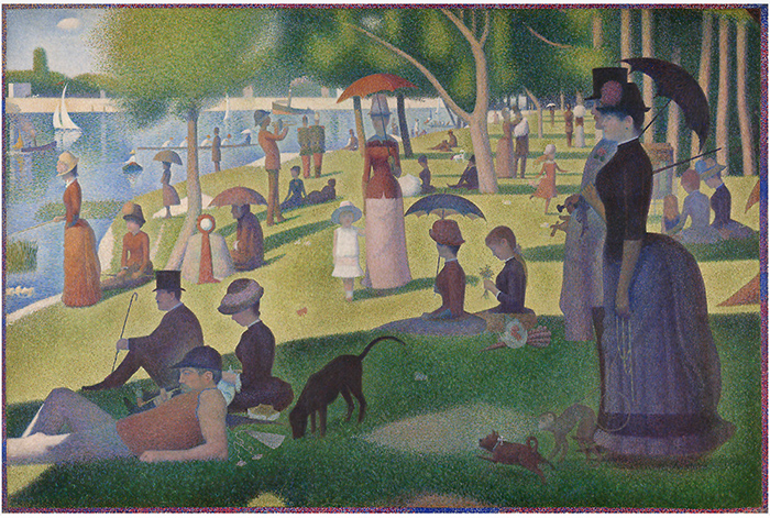 “A Sunday on La Grande Jatte” is probably the best-known example of French painter Georges Seurat’s pointillism technique. Inspired by research in optical and color theory, Seurat juxtaposed tiny dabs of colors that, through optical blending, form a single brilliantly luminous hue. Credit: Art Institute of Chicago (Helen Birch Bartlett Memorial Collection)
 In a recent blog post on Seurat’s website titled, “Seurat’s Origin Story: A Journey from Lab and Lasers to Product and Market,” DeMuth recounts the path that took him from a master’s degree in engineering to the verge of launching a groundbreaking new manufacturing technology.
 James DeMuth
 DeMuth learned about NIF and its cutting-edge mission at a winter 2009 Stanford seminar. “Needless to say, I was captivated,” he writes.
He joined LLNL that June and went to work designing the reaction chamber for an inertial fusion energy (IFE) powerplant. The plan was to capture the energy from laser-driven fusion reactions and turn it into clean, safe, and virtually unlimited electricity.
“The chamber…needs to be able to withstand intense temperature swings and transfer the energy out of the chamber to make electricity,” DeMuth writes. “The space essentially needs to house a sun.”
DeMuth and his colleagues determined that the only material able to handle the 600°C (1,100°F) heat and rapid temperature fluctuations without cracking was a steel-nanoparticle composite able to maintain its strength at high temperatures.
“Unfortunately, this material was unweldable,” DeMuth writes. “This was a big problem since the chamber needed to be 12 meters across. The walls themselves needed to be two meters thick, and with lots of internal structures, they could only be made by welding smaller sections together to make the whole structure.”
The researchers concluded that the only process capable of producing the specialized parts for the reactor was a type of additive manufacturing called laser powder bed fusion (L-PBF). Also known as selective laser melting, L-PBF works by shining a laser onto a thin layer of metal powder; the intense laser spot melts the powder and welds it to the layer below.
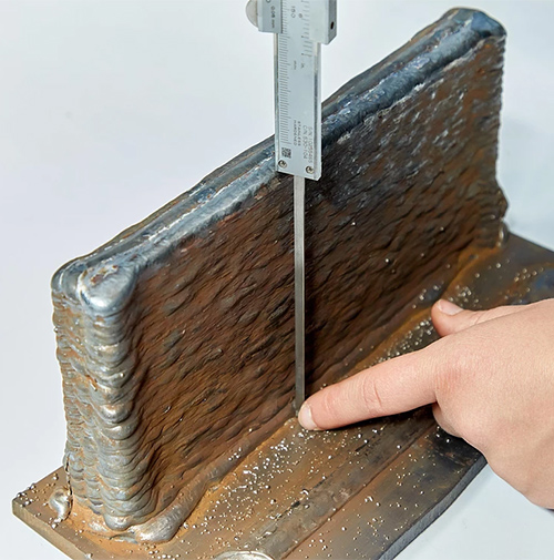 High-deposition-rate AM techniques can produce many kilograms of material per hour, but with vastly reduced resolution. The tradeoff between build rate and resolution is a fundamental limitation of scaling conventional metal AM.
 “The problem with L-PBF, however, is that it is extremely slow,” DeMuth writes. “The fastest available machine in the world, even today, would take nearly 200 years to print just a single fusion chamber at the resolution needed.
“This problem drove me, along with my co-inventors Bassem El-Dasher, Andy Bayramian, Joe Farmer, and Sharon Torres, to work to understand the fundamental barrier preventing additive manufacturing from scaling,” DeMuth writes. “Together, we figured out how to remove that barrier and devised a system that could scale to have a high enough throughput to manufacture these chambers in a reasonable timeframe.”
The solution was to make it possible for every pixel in the laser to function as an individual laser. And as it turned out, a way to do that was already being developed at LLNL.
The key was a device called an optically addressable light valve (OALV), which contains a liquid crystal cell and photoconductive crystal in series. The OALV originally was designed for and installed in NIF as part of the LEOPARD (Laser Energy Optimization by Precision Adjustments to the Radiant Distribution) system. LEOPARD consists of 48 customized “programmable spatial shapers” installed in the preamplifier modules at the front end of the NIF laser system, allowing the NIF laser beam to be patterned with high-resolution images that could be programmed to block or let light through each one of its pixels.
LEOPARD was deployed in 2010 and won an R&D 100 award in 2012. In NIF, the OALV is used to optimize the profile of the laser beams and locally shadow and protect optics subjected to higher intensities and fluences, or energy densities.
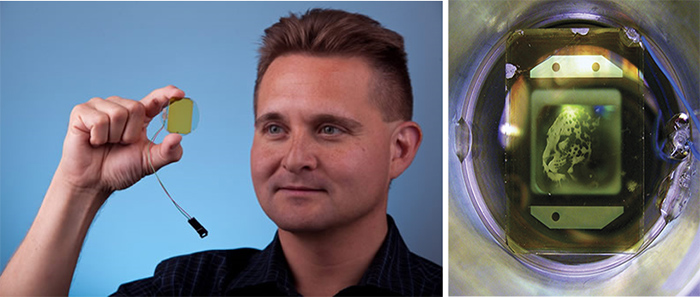 (Left) NIF&PS researcher John Heebner, who led the development of the optically addressable light valve; the OALVs are in each of the 48 programmable spatial shapers forming the NIF LEOPARD system. (Right) An image mask using a leopard photo created by a NIF programmable spatial shaper demonstrates the system’s high resolution and flexibility.
 “Every pixel in the OALV defined its own laser spot,” DeMuth writes, “effectively creating a multitude of individual lasers out of one very powerful laser. Over the next five years, I worked to develop a 5-kilowatt laser system to incorporate a NIF OALV.”
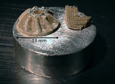 First demonstration of DiAM wide-area photolithographic printing of metal layers using an OALV. For each build—an impeller (left) and an LLNL logo—successive layers were built using a stitching approach which allowed additional efficiency to be achieved.
 In 2013, LLNL’s Directed Research and Development (LDRD) program funded a strategic initiative to develop diode-based additive manufacturing (DiAM), an L-PBF technique that can flash-print an entire layer of metal powder at a time. The DiAM research was led by Chris Spadaccini, Bassem El-Dasher, and DeMuth. Using high-powered arrays of laser diodes, a Q-switched (pulsed) laser, and the OALV, DiAM was able to 3D-print metal objects faster than ever before.
A follow-on LDRD program led by LLNL scientist Ibo Matthews funded wide-area photolithographic printing research. The Lab’s Gabe Guss and Reggie Drachenberg played a central role in producing the parts for the project, with contributions from Josh Kuntz and Eric Duoss.
“This system demonstrated that we could project laser light down to a bed of metal powder, weld a patterned area in an instant, and build a multi-layer part using this technique,” DeMuth writes.
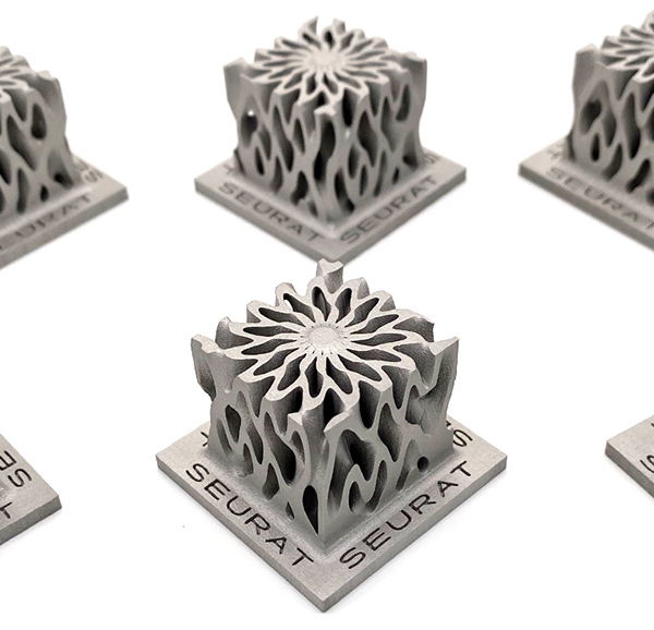 Examples of precision 3D-printed stainless steel using Seurat’s patented additive manufacturing Area Printing technology.
 “This system architecture was the solution, opening endless possibilities for additive manufacturing. With this technique, the ability to operate with millions of laser spots in parallel became possible. Printed feature resolution was no longer tied to the overall laser beam size. Instead, resolution and laser power could be separately engineered to satisfy the requirements of the system.
“Finally, we decoupled resolution from throughput.”
DeMuth and co-founder Erik Toomre formed Seurat shortly after the DiAM technique was demonstrated. Patents for DiAM were licensed to Seurat in 2016 and the company set about fundraising and commercializing the technology.
About four months ago, Seurat demonstrated printing stainless steel with mechanical properties that exceed industry standards, “proving that Area Printing not only can print beautiful parts but can also create quality metal,” DeMuth writes. “Seurat is now scaling to deliver product and bring about a new age of manufacturing.”
More Information
“Diode-based additive manufacturing of metals using an optically-addressable light valve,” Optics Express, May 10, 2017
“Lawrence Livermore discovery a ‘big step forward’ for metal 3-D printing process,” LLNL News Release, May 25, 2016.
“Denudation of metal powder layers in laser powder bed fusion processes,” Acta Materialia Online, May 20, 2016
—Charlie Osolin
Follow us on Twitter: @lasers_llnl


